ANALOG
TO DIGITAL CONVERTER
ADC0808/ADC0809 is an
8 channel 8-bit analog to digital converter.
Conversion Delay
Time taken by the ADC from the Active Edge of Start of
Conversion (SOC) pulse till the Active Edge of (Start of Conversion) EOC pulse.
Algorithm:
·
Ensure
the stability of anolog input applied to ADC.
·
Send the
SOC pulse to ADC.
·
Read EOC
signal to mark the end of the conversion process.
·
Read
Digital output of the ADC as equivalent digital output.
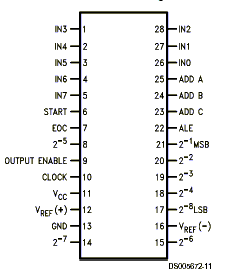
Pin Configuration of
ADC 0808
·
Analog Input (IN0 to IN7)
These pins are eight different analog input.
Each of these inputs is converted to an 8-bit equivalent digital one by one not
all at a time.
·
Address
pins (ADD A, ADD B, ADD C)
These pins select input
of the eight analog input for A to D conversion.
Address
|
Analog Input
|
||
C
|
B
|
A
|
|
0
|
0
|
0
|
IN 0
|
0
|
0
|
1
|
IN 1
|
0
|
1
|
0
|
IN 2
|
0
|
1
|
1
|
IN 3
|
1
|
0
|
0
|
IN 4
|
1
|
0
|
1
|
IN 5
|
1
|
1
|
0
|
IN 6
|
1
|
1
|
1
|
IN 7
|
·
ALE
(Address Latch enable)
This pin is use to
enable the address latch which is store the addresses on the line A, B, C
·
Output
Enable
This pin is use to
enable the digital output on the output lines.
·
2-1
to 2-8 (Digital Outputs)
These pins are used to
provide digital outputs. 2-1 represents the MSB and 2-8
represents the LSB.
·
SOC
(Start of Conversion)
To enable the start
input to begin the A to D conversion. A pulse is to be given on SOC pin to
start conversion.
·
EOC
(End of conversion)
The end of the
conversion is indicated by EOC output.
·
Vcc
This pin is used to
provide supply of 5 V.
·
GND
This pin is used to
provide ground to the supply
·
Vref
(+) and Vref (-) (Reference voltages)
These
pins are used to provide positive reference voltage or negative reference
voltage depending on the desired polarity of reference voltage.
Interfacing ADC 0808 to 8051
·
ADC 0808 has eight input channels. Hence
in order to select an input channel, it essential to send 3 bit address on ADD
C, ADD B, ADD A inputs.
·
The address of the desire channel is
sent to the address input through port pins P2.0, P2.1 and P2.2.
·
After 50 nSec the address must be
latched. It can obtained by sending ALE signals.
·
After 2.5 µSec, SOC must be high and
then low to start to start conversion.
·
To indiacate the end of the conversion
EOC must be activated.
·
The 8051 pins P2.6 and P2.7 are
connected to SOC and EOC pins of ADC 0808.
·
After the conversion is over, 8 bit
digital data is present on D0 to D7 lines. · 8051 accept this 8-bit converted digital
data through port 1.


No comments:
Post a Comment