Showing posts with label FMA Unit 5. Show all posts

Friday, March 22, 2019

FMA Unit 5.7 Interfacing DAC to 8051


DIGITAL TO ANALOG CONVERTER

DAC0808 is an 8 channel 8-bit digital to analog converter.

Pin Configuration of DAC 0808


     ·        Digital Input (A1to A8)
These pins are eight digital input lines with A1 as MSB and A8 as LSB.
     ·        Anolog Outpurt (Io)
         This pin is used to provide analog output in the form of current Io. Therefor                  there  is a need of external current to voltage converter if analog output in the                 form of     voltage is required.
     ·        VEE
This pin is used to provide supply of 15 V.
     ·        GND
This pin is used to provide ground to the supply
     ·        Vref (+) and Vref (-) (Reference voltages)
These pins are used to provide positive reference voltage or negative reference voltage depending on the desired polarity of reference voltage.


Interfacing DAC 0808 to 8051


     ·        The output of DAC is a current which is converted into voltage using OPAMP                based Current to Voltage converter.
     ·        The analog output current Io of DAC depends on the Iref flowing into the Vref              terminal and the status of the D0 – D7 bits.
      It can be expressed as,


Questions              
Write a program to generate triangular waveform using DAC.
Draw 8051 based system to interface DAC. Write a program to generate triangular wave

Write an assembly language program to generate triangular waveform using DAC interfaced with 8051 microcontroller

Interface DAC 0808 with 8051 Microcontroller. Write program to generate sawtooth waveform.

FMA Unit 5.6 Interfacing ADC to 8051


ANALOG TO DIGITAL CONVERTER
ADC0808/ADC0809 is an 8 channel 8-bit analog to digital converter.

Conversion Delay
Time taken by the ADC from the Active Edge of Start of Conversion (SOC) pulse till the Active Edge of (Start of Conversion) EOC pulse.
Algorithm:
·        Ensure the stability of anolog input applied to ADC.
·        Send the SOC pulse to ADC.
·        Read EOC signal to mark the end of the conversion process.
·        Read Digital output of the ADC as equivalent digital output.


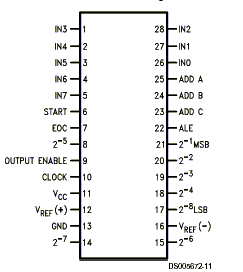
Pin Configuration of ADC 0808


     ·        Analog Input (IN0 to IN7)
These pins are eight different analog input. Each of these inputs is converted to an 8-bit equivalent digital one by one not all at a time.
     ·        Address pins (ADD A, ADD B, ADD C)
These pins select input of the eight analog input for A to D conversion.
Address
Analog Input
C
B
A
0
0
0
IN 0
0
0
1
IN 1
0
1
0
IN 2
0
1
1
IN 3
1
0
0
IN 4
1
0
1
IN 5
1
1
0
IN 6
1
1
1
IN 7

     ·        ALE (Address Latch enable)
This pin is use to enable the address latch which is store the addresses on the line A, B, C
     ·        Output Enable
This pin is use to enable the digital output on the output lines.
     ·        2-1 to 2-8 (Digital Outputs)
These pins are used to provide digital outputs. 2-1 represents the MSB and 2-8 represents the LSB.
     ·        SOC (Start of Conversion)
To enable the start input to begin the A to D conversion. A pulse is to be given on SOC pin to start conversion.
     ·        EOC (End of conversion)
The end of the conversion is indicated by EOC output.
     ·        Vcc
This pin is used to provide supply of  5 V.
     ·        GND
This pin is used to provide ground to the supply
     ·        Vref (+) and Vref (-) (Reference voltages)
These pins are used to provide positive reference voltage or negative reference voltage depending on the desired polarity of reference voltage.


Interfacing ADC 0808 to 8051


     ·        ADC 0808 has eight input channels. Hence in order to select an input channel, it            essential to send 3 bit address on ADD C, ADD B, ADD A inputs.
     ·        The address of the desire channel is sent to the address input through port pins                P2.0, P2.1 and P2.2.
     ·        After 50 nSec the address must be latched. It can obtained by sending ALE signals.
     ·        After 2.5 µSec, SOC must be high and then low to start to start conversion.
     ·        To indiacate the end of the conversion EOC must be activated.
     ·        The 8051 pins P2.6 and P2.7 are connected to SOC and EOC pins of ADC 0808.
     ·        After the conversion is over, 8 bit digital data is present on D0 to D7 lines.                ·    8051 accept this 8-bit converted digital data through port 1.


FMA Unit 5.5 Interfacing of 8051 with 8255 for expanding of IO


Interfacing of 8051 with 8255 for expanding of I/O
·        The interfacing the external memory to 8051, port 0, port 2 are used as multiplexed address/data bus and higher order address bus.
·        If the circuit requires interrupt or I/O then port 1 is only available for this purpose.
·        Hence, in such situations it becomes essential to increase the I/O handling capacity.
·        The I/O expansion is possible twit the help of 8255 PPI.
·        The figure shows the expanded I/O ports using 8255. 
      The data bus is connected to port 1.


Que: Draw and explain with schematic diagram hardware interfacing of 8255 with 8051 microcontroller.

Monday, March 18, 2019

FMA Unit 5.4 8255_PPI_operating modes


8255 Operating Modes
     1.     Bit set reset (BSR) mode – This mode is used to set or reset the bits of port C only. This mode affects only one bit of port C at a time because, as user set the bit, it remains set until and unless user changes it.

Bit D7: 0 for BSR mode and

    1 for I/O mode.

Bit D6, D5 and D4: Don’t care bits
Bit D3, D2 and D1: Port C bit select Bit
D3
D2
D1
Bit
0
0
0
Bit 0
0
0
1
Bit 1
0
1
0
Bit 2
0
1
1
Bit 3
1
0
0
Bit 4
1
0
1
Bit 5
1
1
0
Bit 6
1
1
1
Bit 7
Bit D0: 0 for reset and
    1 for set
2. Input/output mode (I/O) or Control word register
 – This mode is selected when the most significant bit (D7) in the control register is 1.
·         Mode 0 – Simple or basic I/O mode:
Port A, B and C can work either as input function or as output function. The outputs are latched but the inputs are not latched.
It has interrupt handling capability.
·                   Mode 1 – Handshake or strobbed I/O:
In this either port A or B can work and port C bits are used to provide handshaking.
The outputs as well as inputs are latched.
It has interrupt handling capability.
Before actual data transfer there is transmission of signal to match speed of CPU and printer.
·                   Mode 3 – Bidirectional I/O:
In this mode only port A will work, port B can either is in mode 0 or 1 and port C bits are used as handshake signal.
The outputs as well as inputs are latched.
It has interrupt handling capability.

D7
D6
D5
D4
D3
D2
D1
D0
1
GA Mode
PA
PCU
GB Mode
PB
PCL

Bit D7: Mode selection

0 for BSR mode and

1 for I/O mode.

Bit D6 and D5: Group A Mode Selection

                        00 for Mode 0

                        01 for Mode 1

                        0x for Mode 2

Bit D4: Group A port A (PA7 – PA0)

                        0 for output and

1 for input

Bit D3: Port C upper (PC7 – PC4)

                        0 for output and

1 for input


Bit D2: Group B Mode Selection

                        0 for Mode 0

                        1 for Mode 1

Bit D1: Group B port B (PB7 – PB0)

                        0 for output and

1 for input

Bit D0: Port C lower (PC3 – PC0)

                        0 for output and

1 for input